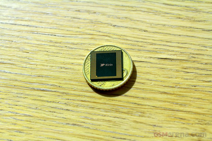
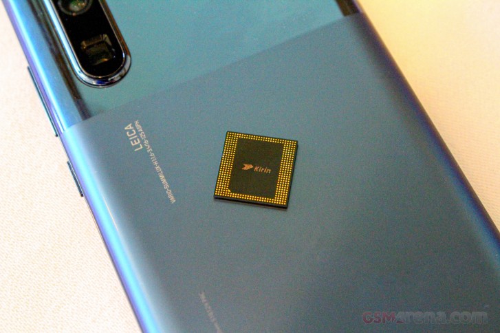
As per tradition, Huawei announced its next-generation mobile SoC called HiSilicon Kirin 990. It's still built on the 7nm process but slightly improved for better efficiency. The chipset uses the brand new 7nm FinFET Plus EUV node by TSMC and it's important to note that Apple's upcoming A13 chip uses the same manufacturing process.
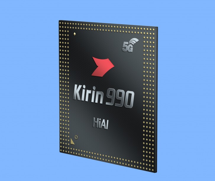
Huawei is boasting many firsts in its flagship mobile SoC. Even though Samsung already announced its integrated 5G-capable SoC, the Exynos 980, the first one on the market is expected to be Huawei's Kirin 990. Up until now, the 5G-capable chipsets were all with 5G modems slapped on the SoC, while the Kirin 990 comes with an integrated modem on board - as a true SoC should be. This ensures more optimized power consumption and less RAM usage. It's also the first SoC with more than 10.3 billion transistors.
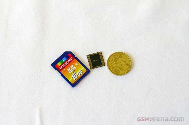
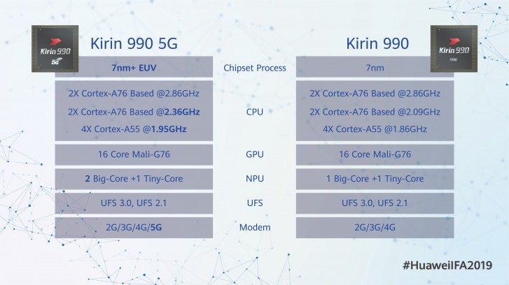
The company promises that its Kirin 990 is the most powerful and the most compact system on a chip today. It's supposed to be 26% smaller than Qualcomm's Snapdragon 855 and 36% smaller than Samsung's Exynos 9820. At the same time, the processor inside makes use of 8 cores - 2x big Cortex-A76 @2.86GHz, 2x middle Cortex-A76 @2.36GHz and 4x small Cortex-A55 @1.95GHz that should outperform the Snapdragon 855 by 10% in single-core tests and 9% in multi-core scenarios. The results below are from Geekbench.
Moreover, the 7nm+ EUV process has allowed Huawei to optimize the power efficiency further and compared to Qualcomm's solution, the Kirin 990 offers 12% better Big-Core efficiency while the middle and little cores stand at 35% and 15% gains, respectively.
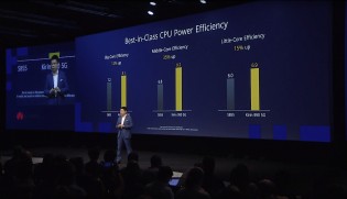
Performance and efficiency comparison with the Snapdragon 855
For graphically-intensive tasks, the same Mali-G76 GPU form the previous Kirin 980 is on board but this time with 6 more cores making for 16 in total. It offers smart cache for games. This way the GPU to DDR bandwidth is improved by 15% while the DDR's power consumption is reduced by 12%. The end result is 6% better graphics performance than the Adreno 640.
Moving on to the AI part, Huawei is making some big gains there too. The quad-core NPU on board is built on the new Da Vinci Architecture, improving performance and efficiency at the same time. It uses the same logic as the standard CPUs in today's SoCs - Big-Core for AI-demanding tasks and Tiny-Core for not as intensive AI computation.
Huawei says that the NPU is so powerful that you can render real-time videos based on the new Real-Time Multi-Instance Segmentation. Interestingly, the 5G variant will be equipped with dual Big Core + Tiny core configuration for the NPU while the non-5G SoC will settle for a single Big Core + Tiny Core setup.
In addition to its own HiAI platform, the NPU can also work with Facebook's Tensorflow and Google's Android NN platforms.
The NPU has also been put to work with the ISP for better image quality and additional features as well. One of them is the Dual-Domain video and photo noise reduction. And speaking of video, the chipset is capable of recording 8K HDR videos at 30fps.
To help with processing and power consumption, Huawei also introduced the new Kirin A1 co-processor for dealing with Bluetooth connectivity, ultra low-power applications and audio decoding. It's an independent power management unit.
We expect the chipset to hit the market sometime in October with the new generation of Mates - the Huawei Mate 30 and 30 Pro. Other Huawei and Honor-branded smartphones to follow.
No comments:
Post a Comment